SPLITTER FOR S/PDIF COAX/OPTICAL OUTPUT - WebHTB
SPLITTER FOR S/PDIF COAX/OPTICAL OUTPUT - WebHTB
SPLITTER FOR S/PDIF COAX/OPTICAL OUTPUT - WebHTB

Create successful ePaper yourself
Turn your PDF publications into a flip-book with our unique Google optimized e-Paper software.
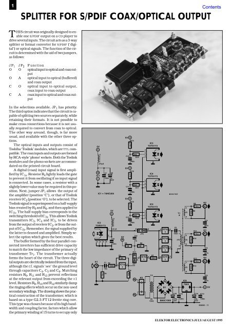
1<br />
<strong>SPLITTER</strong> <strong>FOR</strong> S/<strong>PDIF</strong> <strong>COAX</strong>/<strong>OPTICAL</strong> <strong>OUTPUT</strong><br />
THIS circuit was originally designed to enable<br />
one S/<strong>PDIF</strong> output on a CD player to<br />
drive several inputs. The circuit acts as a 3-way<br />
splitter or format converter for S/<strong>PDIF</strong> (‘digital’)<br />
or optical signals. The function of the circuit<br />
is determined with the aid of two jumpers,<br />
as follows:<br />
JP 1 JP 2 Function<br />
O O optical input to optical and coax output<br />
O A optical input to optical (buffered)<br />
and coax output<br />
C O optical input to optical output,<br />
coax input to coax output<br />
C A coax input to optical and coax output<br />
In the selections available, JP 1 has priority.<br />
The third option indicates that the circuit is capable<br />
of splitting two sources separately, while<br />
retaining their formats. It is not possible to<br />
make cross connections because it is not usually<br />
required to convert from coax to optical.<br />
The other way around, though, is far more<br />
usual, and available with the other three options.<br />
The optical inputs and outputs consist of<br />
Toshiba ‘Toslink’ modules, which are TTL compatible.<br />
The coax inputs and outputs are formed<br />
by RCA-style ‘phono’ sockets. Both the Toslink<br />
modules and the phono sockets are accommodated<br />
on the printed circuit board.<br />
A digital (coax) input signal is first amplified<br />
by IC 1a . Resistor R 4 lightly loads the gate<br />
to prevent it from oscillating if no input signal<br />
is connected. In some cases, a resistor with a<br />
slightly lower value may be required in this position.<br />
Next, jumper JP 1 allows the output of<br />
the amplifier (position ‘C’), or that of Toslink<br />
receiver IC 2 (position ‘O’), to be selected. The<br />
Toslink signal is superimposed on a half-supply<br />
bias created by R 5 and R 6 , and then applied to<br />
IC 1b . The half-supply bias corresponds to the<br />
switching threshold of IC 1b. This allows Toslink<br />
transmitters IC 3 , IC 4 and IC 5 , to be driven<br />
from the output of receiver IC 2 , or from the output<br />
of IC 1b . Remember, the signal supplied by<br />
the latter is cleaned and amplified. Simply select<br />
the option which gives the best results.<br />
The buffer formed by the four parallel-connected<br />
inverters has sufficient drive capacity<br />
to match the low impedance of the primary of<br />
transformer Tr 1 . The transformer actually<br />
forms the heart of the circuit. The three digital<br />
outputs are electrically isolated from the input,<br />
although the r.f. signals ‘see’ the ground level<br />
through capacitors C 4 , C 5 and C 6 . Matching<br />
resistors R 9 , R 11 and R 13 prevent reflections<br />
at the relevant output from exceeding the ×1<br />
level. Resistors R 8 , R 10 and R 12 similarly damp<br />
the ringing effects which occur on the non-used<br />
secondary windings. The drawing shows the practical<br />
construction of the transformer, which is<br />
based on a type G2.3-FT12 ferrite ring core.<br />
This type was chosen because of its high bandwidth<br />
and coupling factor, factors which allow<br />
the primary winding of 15 turns to occupy only<br />
IC2<br />
TORX173<br />
K1<br />
5V<br />
14<br />
L1<br />
IC1<br />
7<br />
270µH<br />
2 4<br />
75Ω<br />
C7<br />
100n<br />
5 6<br />
R1<br />
1<br />
3<br />
C8<br />
1µ<br />
63V<br />
IC1 = 74HCU04<br />
C9<br />
100n<br />
C1 R2<br />
100Ω<br />
10n<br />
5V<br />
L2<br />
47µH<br />
1<br />
5V<br />
R3<br />
10k<br />
IC1a<br />
1<br />
5V<br />
R5<br />
1M<br />
10k<br />
4Ω7<br />
R4<br />
R14<br />
8k2<br />
C10<br />
R15<br />
100n<br />
5V<br />
2<br />
4Ω7<br />
R16<br />
8k2<br />
C11<br />
R17<br />
100n<br />
5V<br />
4Ω7<br />
R18<br />
8k2<br />
C12<br />
R19<br />
100n<br />
C2<br />
O 1<br />
JP1<br />
C<br />
1n<br />
R6<br />
1M<br />
3<br />
JP2<br />
3<br />
2<br />
4<br />
3<br />
2<br />
4<br />
3<br />
2<br />
4<br />
O A<br />
A<br />
IC3<br />
TOTX173<br />
1<br />
IC4<br />
TOTX173<br />
1<br />
IC5<br />
TOTX173<br />
1<br />
5<br />
9<br />
11<br />
IC1c<br />
1<br />
IC1d<br />
1<br />
IC1e<br />
1<br />
R7<br />
IC1b 4<br />
13 IC1f<br />
220Ω<br />
1<br />
1<br />
K5<br />
Tr2<br />
9V<br />
1VA2<br />
B1<br />
6<br />
8<br />
10<br />
12<br />
B80C1500<br />
zie tekst<br />
*<br />
see text<br />
*<br />
siehe Text<br />
*<br />
voir texte<br />
*<br />
C3<br />
100n 1<br />
C16<br />
470µ<br />
25V<br />
Tr1<br />
*<br />
(15)<br />
2<br />
C15<br />
100n<br />
3<br />
(3)<br />
4<br />
5<br />
(3)<br />
6<br />
7<br />
(3)<br />
8<br />
IC6<br />
7805<br />
ELEKTOR ELECTRONICS JULY/AUGUST 1995<br />
220Ω<br />
220Ω<br />
220Ω<br />
R9<br />
75Ω<br />
R8<br />
R11<br />
75Ω<br />
R10<br />
R13<br />
75Ω<br />
R12<br />
C14<br />
10µ<br />
63V<br />
C13<br />
K2<br />
K3<br />
C5<br />
47n<br />
K4<br />
100n<br />
C4<br />
47n<br />
C6<br />
47n<br />
5V<br />
954045 - 11
about half the core, while the secondary<br />
windings of three turns each are distributed<br />
over the remainder. All windings<br />
are made from 0.5-mm dia (24 SWG)<br />
enamelled copper wire.<br />
The power supply is conventional and<br />
‘on board’, consisting mainly of a 1.2-VA<br />
mains transformer, a bridge rectifier and<br />
a 7805 three-pin voltage regulator. All ICs<br />
on the board have individual supply decoupling<br />
parts. Current consumption of<br />
the circuit is of the order of 70 mA. We<br />
regret that the printed circuit board shown<br />
is not available ready-made.<br />
Parts list<br />
Resistors:<br />
R 1 ;R 9 ;R 11 ;R 13 = 75Ω<br />
R 2 = 100Ω<br />
R 3 ;R 4 = 10kΩ<br />
R 5 ;R 6 = 1MΩ<br />
R 7 ;R 8 ;R 10 ;R 12 = 220Ω<br />
R 14 ;R 16 ;R 18 = 4Ω7<br />
R 15 ;R 17 ;R 19 = 8kΩ2<br />
Capacitors:<br />
C 1 = 10nF ceramic<br />
C 2 = 1nF ceramic<br />
C 3 ;C 7 ;C 9 -C 13 ;C 15 = 100nF ceramic<br />
C 4 ;C 5 ;C 6 = 47nF ceramic<br />
C 8 = 1µF 63V radial<br />
C 14 = 10µF 63V radial<br />
C 16 = 470µF 25V radial<br />
Inductors:<br />
L 1 = 270µH choke<br />
L 2 = 47µH choke<br />
Semiconductors:<br />
IC 1 = 74HCU04<br />
IC 2 = TORX173 (Toshiba)<br />
IC 3;IC 4;IC 5 = TOTX173 (Toshiba)<br />
IC 6 = 7805<br />
Miscellaneous:<br />
JP 1 ;JP 2 = 3-way pin header, w. jumper.<br />
K 1 -K 4 = RCA style PCB mount socket,<br />
Monacor T709G.<br />
K 5 = 2-way PCB terminal block, pitch<br />
7.5mm.<br />
B 1 = B80C1500<br />
Tr 1 = G2.3-FT12 ferrite ring core;<br />
primary 15 turns 0.5mm dia. ecw,<br />
secondary 3×3 turns 0.5mm dia.<br />
ecw.<br />
Tr 2 = 9V/1.2VA transformer, e.g, Hahn<br />
BV EI 302 0376; Velleman<br />
1090012M; Monacor VTR1109<br />
(1.5VA); Block VR1109 (1.5VA).<br />
Design by T. Giesberts<br />
[954045]<br />
ELEKTOR ELECTRONICS JULY/AUGUST 1995<br />
954045-1<br />
~<br />
~<br />
954045-1<br />
R14<br />
K5<br />
C10 C11 C12<br />
R15<br />
R16<br />
TR2<br />
R17<br />
R18<br />
IC3 IC4 IC5<br />
8<br />
1<br />
7<br />
R19<br />
B1<br />
<strong>SPLITTER</strong> <strong>FOR</strong> S/<strong>PDIF</strong> <strong>COAX</strong>/<strong>OPTICAL</strong> <strong>OUTPUT</strong><br />
C15<br />
C9<br />
IC2<br />
L2<br />
C16<br />
6 5<br />
C13 C7<br />
L1<br />
C8<br />
C14<br />
IC6<br />
JP2<br />
A<br />
O<br />
R1<br />
C1<br />
C2<br />
R2<br />
R3<br />
R4<br />
R5<br />
R6<br />
R9<br />
R8<br />
4<br />
954045 - 12<br />
2<br />
3<br />
IC1<br />
C<br />
A<br />
O<br />
R7<br />
C3<br />
JP1<br />
C4 C5 C6<br />
R11<br />
R10<br />
K1 K2 K3 K4<br />
R13<br />
R12<br />
TR1<br />
954045-1